

This is another project I did a few years back when I was 20 (in 2012) and managed to sell quite a few units to different organizations. It was using the famous PIC16F877a chip coupled with a DS1307 clock chip (and it’s own battery). This means that this clock wouldn’t lose the track of time even if it wasn’t plugged into a wall outlet for about 10 years. Yes the battery for the DS1307 could last up to 10 years according to the chip’s datasheet.

This model came with an RF remote control as well! you could set the time, date and alarm (yes it had an alarm as well) all by just using the remote control. It wouldn’t forget your settings either since the settings would be copied into the flash memory of the said microchip upon exiting the ‘settings menu’. All of the settings could be set with 4 simple buttons.

In this blog, we will talk about:
1. Main features.
2. What’s inside?
3. What’s on the outside?
4. How does it operate?
5. Circuitry and PCB Design?
6. What’s In the Code?
7. Final Words.
1. The Main Features of This Clock:
It can remember the time up to 10 years even if it’s not plugged in to a wall outlet.
It has an 315mHz remote control for setting the clock - allows the Alarm to be turned off from another room.
It shows the Persian Date (Shamsi Calendar).
It shows the weekdays (in Persian) as well as room temperature.
Battery-less operation. It uses a 9V power supply.
External ICSP connector for updating the program without the need to open casing.
12H and 24H display of time.
Alarm Clock.
Fully scalable and Modular design (Modular PCB Design).
2. What's Inside the Clock?

As you can see the inside of this clock is a bit more organized in comparison to my previous project which was a power supply without a microcontroller. This is because this project was meant to be produced and sold to many customers. Therefore it had to be very neat to make production easy.
This wasn’t the first time I was designing PCBs but I was surely a beginner still. This is the second design of this PCB set. The first set was a double-layer design that was costly to print. So I had to design this single layer version and still maintain similar dimensions to the first set so it fits within the frame. There’s no silkscreen print nor green print at the back. I knew where to put the components. And to save the tracks, I used plastic paint at the back of the boards after the components were soldered.

TIME & DATE MODULES

This is an interesting part of the PCB Design. If you’ve noticed, the PCB for both the Date and clock displays is the same PCB. the function can be different according to the components and jumpers installed! this can greatly reduce the manufacturing costs and make this product even more suitable for mass production!
Each of the 7-segments have a CD4543 Driver in which restores a number inside until it’s refreshed again. There’s no multiplexing of 7-segment pins in here. So they turn on as bright as they can. The ‘CD4543’s adjust their brightness according to the 9v supply voltage.
The AM/PM set of LEDs are controlled by a CD4543 as well! the PIC microcontroller would load a number to that CD4543 and if I remember correctly, number 5 would show AM and number 4 would show PM. I had to go through the outputs of the CD4543 to see which numbers are suitable for this action.
I’ve been thinking about making a clock with Western date & weekdays as well. Maybe that will be the follow up blog to this one? I guess your likes on this blog will determine that.
THE WEEKDAYS MODULE


This will show the weekdays. In Persian, we count the weekdays and we have a Friday. So Saturday is the beginning of the week (yes people go to work on Saturdays and Sundays) which is called “shanbeh”. Sunday is “Yek Shanbeh” (1 Shanbeh). Monday is “Do Shanbeh” (2 Shanbeh) and so on. The only holiday (weekend) is Friday.
So this text shows Shanbeh with the respective number of the weekday for Sunday to Thursday. And it turns the digit off for Saturday and Friday. Just shows the text.

The LEDs are controlled by two wires. One for “شنبه” and one for “جمعه”. The weekdays digit is controlled by another CD4543. Basically the microcontroller updates all of the digits all at once. and writes to all of the CD4543s using a BCD bus and and a few CD4017 which enabling and disabling the latch pin of each CD4543. More on that later in the circuitry and programming sections.
THE TEMPERATURE MODULE


This module was perhaps the easiest of all to design. Just two simple 7-segments and CD4543s. the CD4543s are controlled by a BCD that is available to the board and their latch is controlled by the CD4017 of another board. The Degrees Centigrade Sign is always on.
THE MOTHERBOARD MODULE


The motherboard module was quite an feat to pull off for me at the time. Because it was needed to house the Power regulator, the RS1307 clock chip, the 315mHz RF Module and it’s Decoder as well as the Microcontroller chip with minimum interference from the power side to any of these other chips.
The black wire is used for connecting the temp sensor “DS18S20”. There’s a flat wire that connects the four-button back panel to the microcontroller. And last but not least, there’s a shielded wire that goes to the ICSP socket on the body of the unit.
The first version of this motherboard was a double sided board. But then again, because I needed to reduce the costs as it was a low-production project, it was made into a single-sided board later. which is what you just saw above. The original motherboard looked like below:

THE BUTTONS AND DS18S20 MODULES

Here you can see the buttons used to control the panel that can be accessed through the back of the clock (set the settings) and the DS18S20 installed on a PCB. yes the PCB isn’t a designed one. It’s a Veroboard. I didn’t find it necessary to design a PCB board for a sensor ;)
OK. I think we’ve covered all of the PCB modules here. At the time of the design, I had thought about making SMT PCB modules instead. But then again, soldering SMD isn’t as easy as Through-hole boards for a hand soldering production. So that’s why I went with the older Through-hole.
3. What’s on the outside?


It can show you the Time in both 12/24h formats. It can show the Persian date (Western date can be shown but an update through the ICSP port is necessary). The settings can be set through the remote control as well as the buttons at the back of the display and it uses 9VDC, 1A to operate. I don’t have a picture of the power supply though. I remember I had to ask a printing company to cut the layout of the display on a black sticker in which I would apply onto a glass later.
Applying the adhesive sticker was quite easy. I used to make the glass wet, and then paste the big sticker all at once. Then, because of the wetness, I could easily adjust the sticker to make it match the corners of the glass. Once I was done with the adjustment, I would then use a ruler to even the surface of the sticker on the glass and let out all the water underneath it. Then I kept the glass somewhere warm where the water under the sticker would vaporize completely and let the sticker stick firmly. So what you see in the picture above, is actually the back of the sticker. One could easily clean the glass without hurting the sticker (because it’s at the back of the glass). It was fun to do!
The ICSP Socket can be used to easily re-program the clock without having to open the unit. For instance, the western date could be added to this clock so then it will switch back and forth between the Persian date and western one.
4. How does it operate?


Setting the time on this clock is pretty easy. You’d need to press the “select” button to get into settings menu. pressing “select” again would allow you to choose another parameter to set. Pressing “set” would get into that parameter and allow changes by the “Up” and “Down” buttons. Pressing “set” again, would exit setting that parameter. and finally, pressing “select” again would exit the settings menu. This is easy because unlike some other clocks, you don’t need to set every parameter to get to the parameter that you wish to set. you can easily “select” the parameter first and then set it.
This clock can operate (remember the time) without electricity for up to 10 years. That’s right. 10 years! The display of course would turn off. but the counting will continue. so you’ll never have to set it again. This is due to the DS1307 clock chip that uses it’s own battery to operate and keep time when there’s lack of power. So a power trip or moving the clock from one office to another shouldn’t be a concern to the settings at all. Isn’t that great?
Here’s a little snippet of the live clock in action:

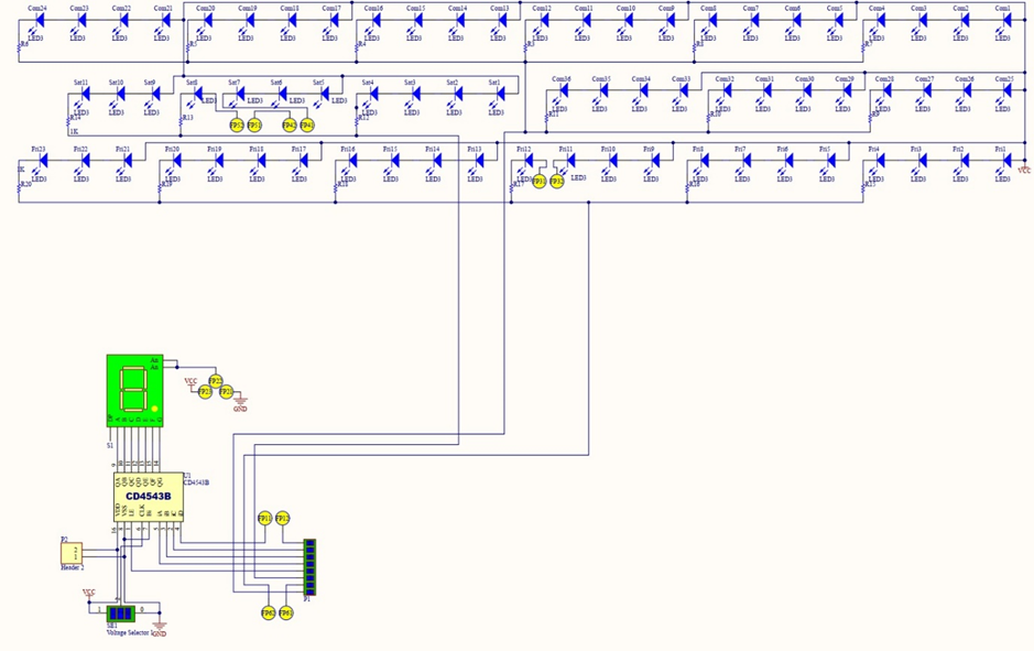
5. The Circuitry and PCB Design?
I will show you the circuitry and PCB design of each module separately so it won’t get too complicated.
Designing the PCBs and coding this project, took me nearly six months. I wasn’t new to coding, but I was new to PCB design. So I took some time in learning the PCB Design as well (that was in 2011). I have yet to design more PCBs to become a professional at it. It’s a joy for me to design. And if you’re a professional PCB designer and design PCBs everyday with Altium, I would love to hear your comments on how to make this design better.
THE MOTHERBOARD MODULE
The motherboard module came in two different versions for the PCB with the same schematic design. First, we’ll take a look at the schematic:


So here, you can see both of the version of this motherboard in detail. the links above include both the Schematic and PCBs. The second version is of course simpler and doesn’t have two AND logic gate ICs as they weren’t necessary to be included on the motherboard.
I had to build all of this circuitry on a breadboard first to make sure it’s functional before proceeding with this print. I had simulated the software in Proteus (Labcenter Electronics) as well. All of the schematics you’re about to see in this blog are created with Protel DXP (altium designer) program. I created them in Altium designer so then I can network them with the footprints on the PCB later on which made the PCB routing much easier. Therefore anything on the schematic has a presence on the PCB as well. The small round yellow circles are footprints that’re created for jumpers. They’re used as individual pads as well. This schematic has been modified quite a few times as the PCB was designed.
There’s a single microcontroller that is receiving information from all of the ICs in this board and sending BCD (binary coded decimal) signals to the display drivers on their respective modules. The microcontroller selects the intended CD4345 through the daisy-chained CD4017s first, and then changes the values on the BCD line that is shared among all of the Digits. It will then send one HIGH clock to the CD4017 and change the BCD value again to write to the next CD4345 and so on.
With this setup of CD4017 and CD4345, you can literally update endless number of numbers on a display for as long as your microcontroller doesn’t run out of memory or the signal on the BCD line hasn’t died (because of the eventual length of wires). The great thing about this method is that you don’t even need to use a full port of your microcontroller. The BCD line will take 4 pins, the CLOCK pin of the daisy chained CD4017s will take another and their RESET pin will take one more pin. So a total of 6 pins can control endless number of displays. Isn’t that cool?
In this motherboard, the microconroller receives a signal from the remote control decoder in the dacade form. For each button, there’s an assigned pin that goes High in case it’s been activated by the remote control. I’ve put a few jumpers there so in case a remote control’s button setting was different, I could change the jumpers on my motherboard and UP wouldn’t become DOWN for the customer. These inputs are shared by the 4-button-module as well. Which is why you can see there’s a diode in series with the output of the remote control decoder chip. This is to prevent backwards current to the decoder chip if the buttons are pressed.
The DS1307 is connected to the Motherboard through an I2C connection. the DS1307 basically counts and stores all of the values for the clock inside itself. The date and weekdays too! All the microcontroller has to do is to read it and then place the digits in the right display module. The Microcontroller can also write to the memory of DS1307 through the same I2C connection. So this board had two Crystals. One was a 32.768 KHz crystal used for the DS1307. and the other is probably a 20Mhz crystal used for the PIC chip (the microcontroller used was PIC16F877A).
If you’d click on the images of the schematic above, you’d see that I’ve placed a 100nf ceramic cap in between the VDD and VSS of the Microcontroller. This chip albeit looking useless, is actually very crucial for proper operation of the microcontroller. Because, no matter how good your power supply is, your microcontroller is still susceptible to high frequency noises created by surrounding devices… such as when you’d turn on the lap in your room, or when you would use a an igniter to turn on the oven (which creates an arc). Yes, that spark could affect the operation of this microcontroller if this 100nf capacitor isn’t there to cushion the noise. I’ve seen it with my own eyes. I would say both a 100uf cap and a 100nf cap are necessary right at the voltage pins of every microcontroller that is being sold in a commercial product. Heck, you could put a few de-noising coils there too for good measure. After all, your product better work reliably if it’s going to be sold to a customer.
I used a good old-fashioned LM7805 regulator for powering up the microcontroller, the DS1307 and the remote conrol deoceder as well as the receiver module. well, LM7805 wasn’t and isn’t the most efficient regulator on the market (it’s a linear regulator), but it gets the job done. It’s reliable and cheap.
Let’s take a look at the PCB design of the first version vs the second version:


The board on top is the first version and the board underneath is the upgraded or second version. I have figured that by placing the components a little bit better, I could drastically reduce the complexity of the board as can be seen in the second version. Not only that, this board didn’t actually need to be a double sided board. Although double-sided boards have become the standard nowadays, for a simple project like this, a single-sided board is still more cost-effective. Given that all the components used are using a through-hole footprint (for ease of production by hand).
The second PCB has less chips of course. Two AND logic gate chips have been removed as they weren’t necessary for this motherboard. This is because the chips can be placed on the Display/Date modules in the second design.
I used more copper surface area for the GND in the second design and even put a pad right next to the Crystal so then it’s body can be soldered to the GND. That’ll make it immune to outside noise and will let the board operate normally at all times. There’s one soldering pad for the Crystal of DS1307 as well!
PCB design with Altium Designer can be quite fun if you know what you’re doing and you’re fluent with the software.
THE TIME/DATE MODULE
The time and date PCB design was quite interesting because it contained two schematics inside. One for the date and one for the Time & depending on which components are installed, you could get a different module. For instance, if the LEDs of the “slash” are installed with the relevant driver IC and jumpers, then it will be a Date module. And if the semicolons are installed instead, it will be a Time module.
The first doubled sided board design didn’t include 8 digits as you can see below. It only included 6 digits and the other 2 digits for “1390” would be added by the Temperature module that could work as a Digit display as well (more on that later in the blog). However, the second design of this module didn’t need anything extra to be transformed into either a date or time module. Everything was on the board itself. If you wished to make it a Date board (second design), you could install the seven segments at the left end of the PCB, and if you wished to make it a Time board, then you could go ahead with the AM/PM LED text.
Let’s have a look at the Schematics for version 1 & 2. The second design had more LEDs because it included the AM/PM text as well:


This is the schematic for the second version of the Date/Time module. In this design which is similar to the previous board, depending on which jumper or component you install, you could make this module function differently. The LEDs you see in the middle are used to display AM/PM. and the LEDs you see on the left side are used to display the double dot between the time digits or the slash between the date digits. The AM/PM LEDs can be turned on with a transistor array chip “U11”. This chip is also responsible for driving the weekday LEDs in the weekday module. I tried to save on extra transistor while keeping the functionality the same.
There’s a connector on the right side in which the module receives the BCD code from as well as the CLOCK and RESET signals for controlling the CD4017s. You can download the high resolution schematic and the PCB from the link above.
The way this module works is quite interesting. Since the CD4543s can hold a number in their latch mode, you can use a CD4017 to take advantage of them. One CD4017 can manage nine CD4543s and therefore 9 digits (output 0 of the CD4017 is useless because it will always be on when the chip is reset). CD4017 can be used in other areas as well. for instance, if you need to read a large keyboard and you don’t want it to take too many pins of your microcontroller, you can use a daisy chained CD4017 configuration to literally read as many keys as you want. The clock of the CD4017 can operate up to 5mhz if I’m not mistaken. so you could scan them quite fast too!
The microcontroller could count the pulses it’s sending to the CLOCK of the CD4017s and if a button is pressed at for instance 30th pulse, it would know which button that is, according to the table you’ve set inside it. But you’d have to use a CD4017 for every 9 buttons. The downside however, could be that the more buttons you scan in series with this method, the slower the scan could get. and there might be a fan out issue at some point. But you can surely save some pins from your microcontroller. CD4017s are commonly used in text scrolling displays as well for turning on LEDs consecutively.
OK. Let’s take a look at the PCB designs of these modules:


As you can see above, a well designed PCB will always look pretty. My goal in designing this one was to avoid any jumpers that I could and make the unavoidable ones as short as possible. A few of the tracks that are used for power are a bit thicker as you see in the picture above. That is because I had set the minimum width of a power track to be 2mm I think in the design rules for Altium Designer. I tried to get the CD4543s as close as possible to the seven segments. that way the PCB would become smaller. That is why there are long tracks on top of the PCB…
This PCB can house 8 digits and thus has 8 CD4543 driver chips as well as a single CD4017 that is controlling their latch. There’s a Transistor array as well that is used to turn on the LEDs in this module as well as throughout the clock.
As you can see, I’ve put all of the resistors for the AM/PM text in one place so then it’s easier to install them on the board by hand. There are sets of 4 LEDs in series with a resistor that make them quite bright for a 9v display panel.
THE WEEKDAYS MODULE
The weekdays module comes in 2 versions as well. Let’s have a look!

Here, you can see the schematic for the weekdays module. This is the first version and so there are 2 transistors used to turn on the text LEDs. There’s a common set of LEDs that will be turned on by both that is common among the two words for Friday and Saturday (جمعه و شنبه). The common set of LEDs needed an OR gate keep on regardless of which word is being shown. So I used two Diodes to do the trick. It works like an OR gate. So if either transistor is turned on, the common LEDs will turn on too. and if none of the transistors are turned on, there won’t be any light.
This is useful when the panel is turning itself off due to the user pressing the off button. We would need a software switch and this could be considered as a soft switch here. The number panels have a soft switch as well. If you would write a number higher than 9 on the CD4543s, then the 7-seg will go blank. Some CD4543s however, will turn some of the segments on in such case. However, the ‘blanking input’ of the CD4543 will turn off the 7-segment completely. In this design, I haven’t used the blanking input of the CD4543 to turn off the panel in “power off” mode. I have rather used the other function of the CD4543 that was just mentioned and I was careful to choose the Chips that would follow that behavior.
A closer look at the second schematic will help you see that it doesn’t include the transistors that were included in the first design for turning on the text. These transistors were moved to the Clock/Date module (the transistor array).
Let’s have a look at the PCBs. Shall we?


Here we can see that the weekdays module actually doesn’t need to be a double-sided board. With a bit of simplification, a one sided design is just fine. Surely adding another layer can help with the jumper situation. But since these are LEDs one could easily stretch their footprint a bit longer to get headroom for a track to pass through. Which is why we see almost no jumpers on this board.
The second PCB doesn’t have transistors as they are located on the Clock/Date PCB module (the transistor array chip).
THE TEMPERATURE MODULE

The temperature module was perhaps the simplest of all. It included of only two CD4543s and a few LEDs. but this module too, had two versions and the second version was the improved one in which had more LEDs for the Celsius sign. The first design of this module (as can be seen above) was capable of either being an extension to the Time module and show AM/PM text, or work as the temperature display.
When used as an extension, it still needed a CD4543 chip to operate as you can see in the schematic above. That is because I decided to use a chip to lock the text on displaying either AM/PM. It was just easier to load a number into the CD4543 as it’s part of the daisy chained CD4017s compared to dedicate 2 pins of my microcontroller to determine which text should be shown (AM/PM). And it worked very well! specially considering that I could load a number higher than 9 into my CD4543 and have the text turned off when the whole display is turned off by software.
In this way, I could save on two diodes as well by using a segment of CD4543 that turns on in both numbers. Such as the G segment which is on in both digits 4 and 5. Here however, output D was connected to AM (the Leg of A) and output C was connected to PM. I don’t remember what number I used at the time, but maybe that something you can figure out on your own ;).

The first version of the PCB Design for this module is a single sided board as well. If you’d look at the middle bottom of the board, you’d see that there is a pad to select the voltage (negative or positive) for the seven segments COMMON pin and another one to the left of it to select the CLOCK voltage for the CD4543s. This would allow the CD4543s to reverse their output voltage to the seven segments and also the COMMON pin of the seven segments. This makes it possible for the board to use both Common Anode and Common Cathode Seven segments. All of the display modules have been designed this way. So if one is using a common Cathode seven segment or common Anode seven segment, all they have to do is solder either of the pins at the said pad together and the board is set. The CD4543s are able to reverse their output depending on the polarity status of the CLOCK input.

You can download the full schematic and PCB Design of both of these designs for the Temp. module below:
The second design of this module is simpler and doesn’t include the AM/PM text as that is being handled by the Clock/Date display module. But it carries the same attributes and it only does one thing and that is to show the temperature.

THE BUTTONS MODULE
This Module is the simplest of all. Just 4 tactile switches with a long actuator with connected together with a common ground. That’s the easiest way you can read 4 buttons I think.

You can download the Schematic as well PCB file from the link below:
I love modular design. and I tried my best to make this clock scalable and modular. so then if I receive an order with special needs, I can easily adjust the design by just adding or removing a few modules. A friend of mine suggested that I would use one single pcb for all of this but I think that would be a big waste of material and money. The best thing about these modules is that in case I needed to increase the size of the seven segments, all I have to do is to change the seven segment footprint accordingly and print the new PCBs. Everything else about the circuitry and the modules stays the same. So yeah, maybe I would design bigger modules and make a clock for myself! if I have time for that… . I had sold all of the units.
As for the wiring, all of these modules share the same bus line that starts at the top with the Clock display module, goes to down to Date, Weekdays and lastly the temperature module. the bus line has fewer wires when it reaches the temperature module.
6. What’s In the Code?
The coding for this clock took nearly just as much as time as it took for me to design the PCBs. Unfortunately I don’t have the full copy of the code which was the final revision. However, I will discuss some of the important parts of the coding that I was practicing with. I used PIC Basic Pro to program the PIC microcontroller just so the programming becomes easier and I can focus on the other parts of the design better. I could’ve used C as well. But that would’ve taken longer to code.
The challenging parts of the coding for this project was mainly reading/writing data from the clock chip (DS1307) with an I2C protocol as well as reading data from the temperature sensor (DS18S20) using a One Wire protocol. Writing information to the display driver chips (CD4543) for displaying the time, date and temperature was rather easy with the help of the daisy chained CD4017s. And as for the remote decoder, there is literally no programming involved. If you’d have a look at the schematic of the motherboard, you see that it is connected to the button inputs of the microcontroller. So it mirrors the remote control’s buttons with the one one the body of the unit. There is a diode in series with each output of the decoder chip to prevent backwards current to the decoder chip when a user would press the buttons on the unit.
So in this section, I will cover the important code that makes this clock tick:
Global Settings Throughout the Program.
I2C Connection With DS1307 Clock Chip For Reading And Writing Data.
One Wire Connection With DS18S20 Temp. Sensor Chip For Reading Data.
Writing Information Into The CD4543 Seven Segment Driver Chips With The Help Of CD4017 Decade Counter.
GLOBAL SETTINGS THROUGHOUT THE PROGRAM
There were some settings that applied to the entire program. Settings such as defining the Variables (Bytes, words and etc.), the oscillator frequency, I2C type of connection, Alldigital.phb to make all ports digital, modedefs.bas for better operation of PBP, Setting specific pins as input or output and etc.
Here’s a quick look at the Global Settings. There were too many variables that I don’t remember so I haven’t included them.

The configuration code on top of the program is quite essential to avoid complications later on when writing the code. For instance mentioning TrisA = $11000000 will keep two of the pins from port A as inputs and the rest will be considered outputs throughout the entire code. Including modedefs.bas is necessary when using serial communications with other chips and alldigital.php will keep all of the pins in the digital mode and will deactivate the DAC converters. This is necessary if you’re not reading an analogue sensor or sending an analogue signal out of the microcontroller. It will help to keep the ports in digital mode so they don’t get interfered by any of the analog modules inside the microcontroller. If you have worked with PIC microcontrollers before, you would know that it is necessary to configure the ports to “all digital”. Otherwise, the analog modules could be activated by default and cause your port to malfunction.
ADCON1 Controls PortA’s analog modules. You can read more about it in PIC16F877A’s datasheet. I had included the alldigital.php but I was just using assembly syntax just to make sure all ports are digital. It is essential to read the datasheet of the microcontroller you’re programming because of these small little registers that you wouldn’t be able to guess.
I2C CONNECTION WITH DS1307 CLOCK CHIP FOR READING AND WRITING DATA.
Talking to the DS1307 chip is very efficient and simple when we use the commands I2CWRITE for setting the chip and I2CREAD for reading the chip. I2CREAD will be used much more often since this clock needs to show time more than being set (once every 10 years really). But I2CWRITE must be implemented properly into the code.
This chip doesn’t have an Alarm function. But alarm function is pretty easy. You can set an alarm bit that goes 1 if the user has set an alarm. And then set the micro to check the time when it’s read from DS1307 to see whether it matches the alarm time set by user. if it does, it can ring for a minute or two… . That is what I did for this clock. Even though it’s a wall clock and doesn’t need to have “alarm”. I thought it could be done and I was curious enough to do it :)
Anyway, let’s get to the coding part. the I2CWRITE and I2CREAD commands have been used sporadically throughout my code. So it would be useless for me to take a screen shot of them. However, the one on PBP’s website is a good sample program. So this is sourced from melabs.com:

In the code above, we see that I2CWRITE is initially used to write the date into the chip so then it can count further. Then, I2CREAD is used to retrieve the latest time information from the chip. LCDOUT can help to show the information on the LCD Panel. It then PAUSES the whole code for 500ms (half a second) and does the same thing again.
Using a 500ms pause in the code isn’t a good idea in my opinion. You could instead assign a number to a variable, ask the micro to add 1 to it every 50ms for instance and when the number reaches 10 (which means the program has waited 500ms, 10 * 50 = 500) then leave this loop. But during this time, your code isn’t frozen and you could have maybe read the keyboard 10 times during this 500ms PAUSE. Because while the microcontroller is on PAUSE, it won’t do anything else.
ONE WIRE CONNECTION WITH DS18S20 TEMP. SENSOR CHIP FOR READING DATA.
One Wire Connection is a very convenient and simple way of communicating with another chip without having to write too much code (At least not in PBP) or use too many pins.
Let’s have a look at the code for this:

Here we can use OWOUT and OWIN commands to send and receive data to the DS18B20 temp sensor. There is not much data we can send to the sensor other than asking it to convert the temp data into bits or to see whether it’s still busy converting or not. It will then give us the data back as a WORD. It give us a word because the first 4 digits are the “-” and “+” indicator. So if it’s positive temperature, we can use the special multiplication “*/” to truncate the unwanted bits. As they will be 0 anyway. Once we have the real value, then we can put them in two different bytes in which each would be shows on a different seven segment (next to each other).
You can download the DS18B20 Datasheet Here.
I chose to put them into 2 different bytes because that would make it easier to show in the BCD line shared by all of the CD4543s. Sure, I could have used a single byte for 2 digits and then divided them when loading the BCD, but that would’ve made it a bit more complicated.
At the end in this sub loop, the DS18B20 is asked to convert data again. This way, the data is ready to be displayed each time this loop is recalled. And we don’t have to check to see whether DS18B20 has done the conversion or not. Because the microcontroller will be busy doing other things before recalling this sub again. This would make the code just a bit simpler too. It’s not only the right code that makes a device tick. it’s the order of lines too.
You can read more about the coding this temperature sensor at the official PBP site here.
WRITING INFORMATION INTO THE CD4543 SEVEN SEGMENT DRIVER CHIPS WITH THE HELP OF CD4017 DECADE COUNTER.
Writing information into the CD4543s is quite simple. All you need to do is send the appropriate BCD code while the Latch pin is released. When you’re done, you can lock the latch again, open the latch for the the next CD4543 and change the value on the shared BCD line between the two chips. This locking and unlocking the latch pins can happen with a CD4017. A very cheap and yet useful chip. one CD4017 can control the latch of 9 CD4543s. That is because the “0” output of the CD4017 is always on before receiving a clock signal and therefore is quite useless. Specially when we have a bunch of CD4017s in a daisy chain configuration with a CD4081 (quad AND chip). Then all of the “0” outputs in the daisy chain are useless. However, we’re getting 9 other outputs that work fine. so there’s not much to complain about. 2 CD4017s and a CD4081 can control 18 digits. So it’s worth it!. You’ve seen the circuitry for this in the clock/date module. Now take a look at the simple code:

To send a BCD number (Binary Coded Decimal) through our port (so it just uses 4 bits instead of 8 and we can use the rest of the pins for something else), We can add “& $0F” after the variable as you see above. This will get rid of the remaining digits in the byte and send the 4 least significant digits to the port.
PortA.5 had been assigned to the clock of the CD4017s. So everytime this pin is toggled, the next CD4543 is ready to receive data. And if you’re changing the data on only one of the digits, you have to have all of the other variables with the right value ready. Because you’ll be setting all of the other digits as well. The good thing is that the CD4543s won’t blink our 7-seg if you set them with the same data so the users won’t notice.
So as you see, the code is very simple. As mentioned before, the daisy chained CD4017s can be used for a variety of applications. Setting digits as you just saw, reading a keyboard (the keyboard has to have a matching wiring), turn on LEDs in a text scrolling display and etc. That makes this IC very interesting despite its simplicity.
7. Final Words:
This project taught me many new things just as the previous project did. It allowed me to sharpen my coding skills as well as PCB design. I have yet to design more complicated PCBs. But I think this was a good try for a 20 year old (at the time). Electronics is truly an endless field. You’ll never really learn everything in Analog, Digital, High Voltage, Avionics, Telecommunication and etc. So constant learning is a must. And a pleasure too! If you like complicated stuff like I do :)
I’m thinking about creating another version of this clock with both Western and Persian dates. And a Western Weekday module. Then I’ll have the full code and I could share it with you. Please show some love by sharing this blog so I can make that happen.
Long story short, I believe this is how we should learn electronics! Through projects. projects and more projects.
See you in the next one!
Comments